
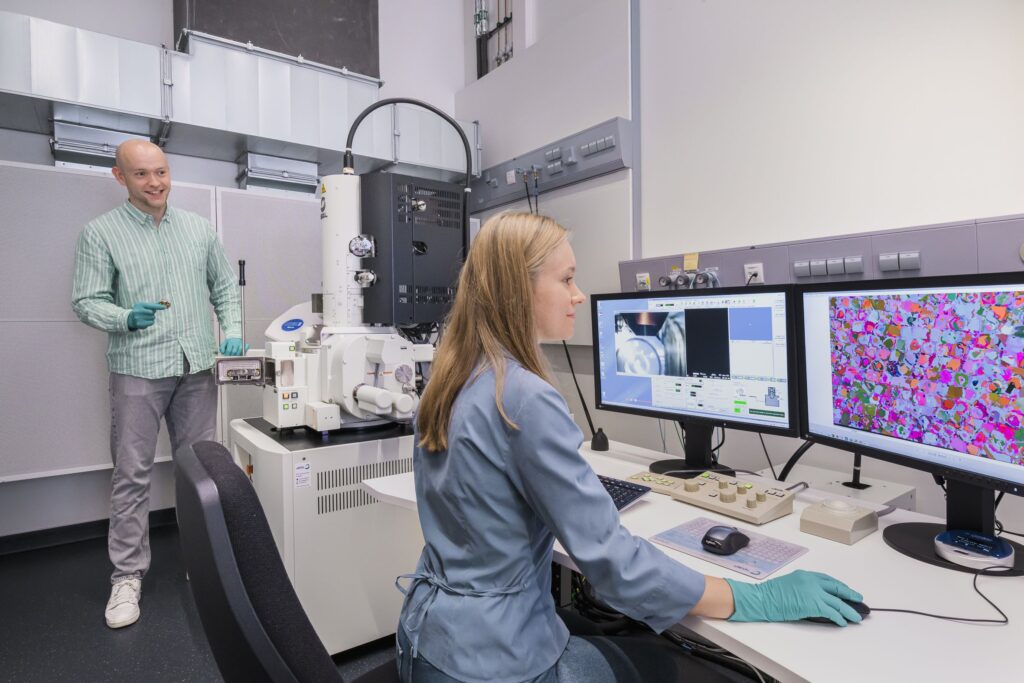
Jeol JSM-7200F
 |
|
Specifications:
- HT: 0.1 ÷ 30 kV
- Max. beam current > 600 nA
- Resolution: 1 nm@30 kV, 1.6 nm@1 kV
- Detectors: SE, BSE, In-lens SE and BSE
- Analytical detectors:
– WDX: Oxford INCAWave 500
– EDX: Oxford AZtecEnergy X-MaxN 80mm2 – SDD
– EBSD/TKD: Oxford AZtecSymmetry CMOS detector
Key features:
- In-lens Schottky FEG
(combines el. gun with condenser, producing large probe current) - Through-the-lens detectors with energy filter
- Aberration correction lens (ACL)
(automatically optimizes both small probe current spot size for high resolution imaging and spot shape for high beam current, high resolution microanalysis) - A beam deceleration mode
(suppress charging on nonconductive specimens) - Field free objective lens
(magnetic samples can be analyzed without restriction) - Airlock
- In-column Faraday cage
- Stage Navigation System
- Wide range specimen holders, including 4 ” wafer sample holder
Applications:
- Imaging (GB’s, interfaces, plastically deformed zones, phases, precipitates, some of planar defects)
- Spectroscopy: EDX, WDX (chemical element identification, mapping, quantification):
- Diffraction (EBSD, TKD: grain analysis, phase identification and mapping, texture assessment, strain maps)